Transistor Capacitances
EEE 131 THX2/Y
2025-11-19
General Frequency Response
Most amplifiers have a frequency response that looks like the following: 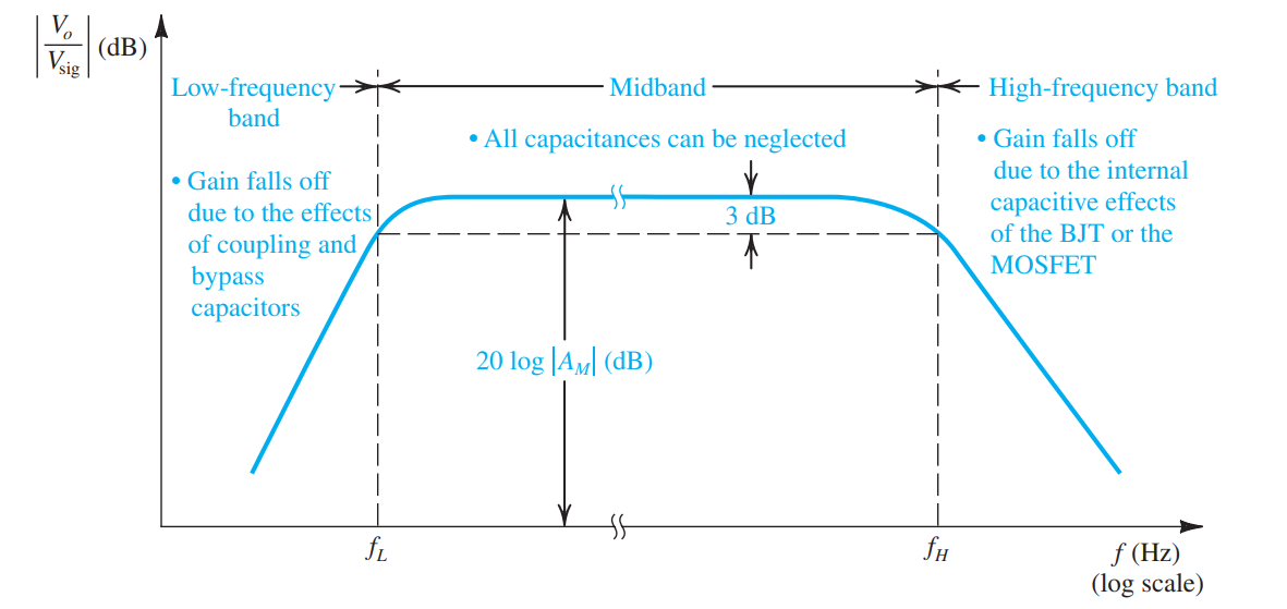
Everything is a capacitor
If something holds charge, it is a capacitor.
\[C = \frac{dQ}{dV} \]
Hence, everywhere in semiconductor devices where there are holes and electrons moving in and out there is capacitance.
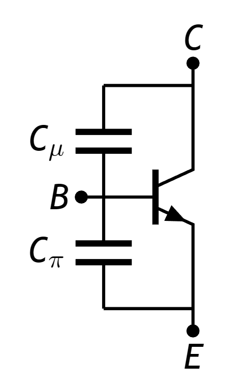
BJT Parasitics
There are two main parasitic capacitances in a BJT:
- Base-Emitter Capacitance \(C_{\pi} = C_b + C_{je}\) (Base Charging Capacitance + Base-Emitter Junction Capacitance)
- Base-Collector Capacitance \(C_{\mu}\)
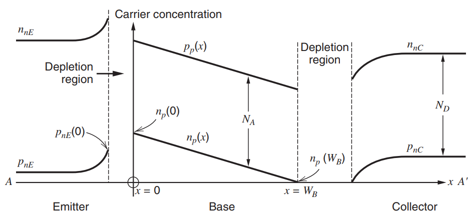
The base charging capacitance \(C_b\)
Before we start using the BJT, there is effectively “no charge” in the base region.
However, as we turn the BJT on, the emitter starts to inject carriers (charge) into the base.
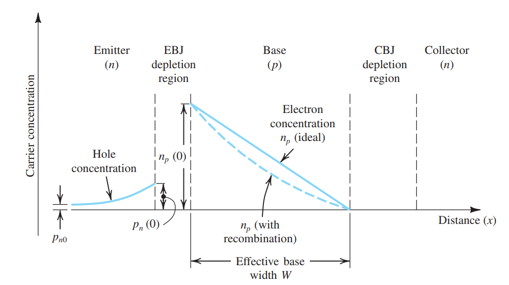
The BE Junction Capacitance \(C_{je}\)
A depletion region is a region with charges.
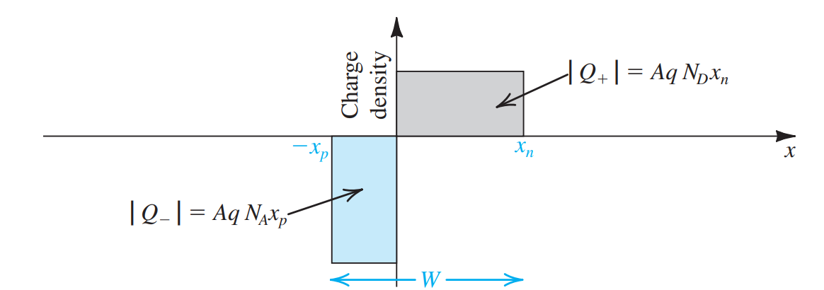
As we discussed before, the width of the depletion region changes with applied voltage. It is known that \(W_{dep} \propto \sqrt{V_{bi} - V_{BE}}\).
The BE Junction Capacitance \(C_{je}\)
\[\frac{C_{je0}}{\sqrt{1 - V_{BE}/V_{j,BE}}}\]

BJT Parasitics Summary
- \(C\mu\) - Junction capacitance between B and C
- \(C_\pi = C_b + C_{je}\)
- \(C_b\) - Capacitance from carriers crossing the base
- \(C_{je}\) - Junction capacitance between B and E
Tip
\(C_\mu\) and is typically around 5fF-10fF.
\(C_{je}\) is a little higher, about \(>10fF\).
\(C_b\) is typically around hundreds of fF.
BJT Small Signal Model with Capacitances
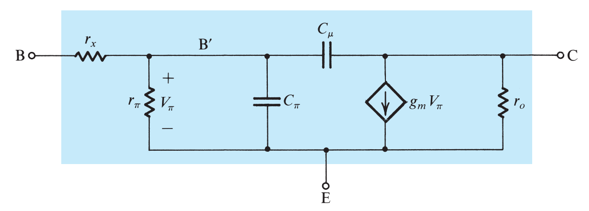
\[C\pi=C_b+C_{je}\] \[C_b=\tau_Fg_m\]
\[\frac{C_{je0}}{\sqrt{1 - V_{BE}/V_{j,BE}}}\]
\[ C_{\mu} = \frac{C_{\mu0}}{\sqrt{1 + V_{CB}/V_{j,CB}}} \]
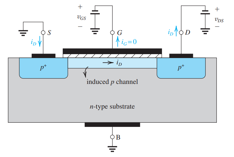
MOS Parasitics
The MOS has three sources of parasitics:
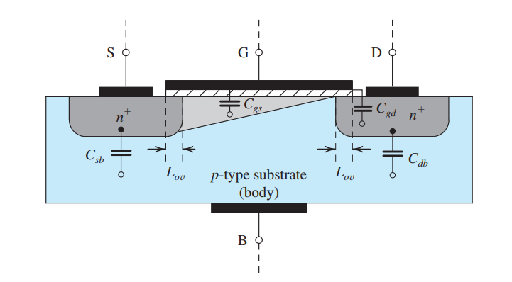
Drain/Source to Bulk Junction Capacitance \(C_{db}\),\(C_{sb}\)
- Same as earlier.Gate-bulk capacitance \(C_{gb}\)
- The MOS Capacitor. Remember this?Gate-overlap capacitance \(C_{gs}\)
- MOS Capacitor but we accidentally do it to S/D.
MOS Parasitics
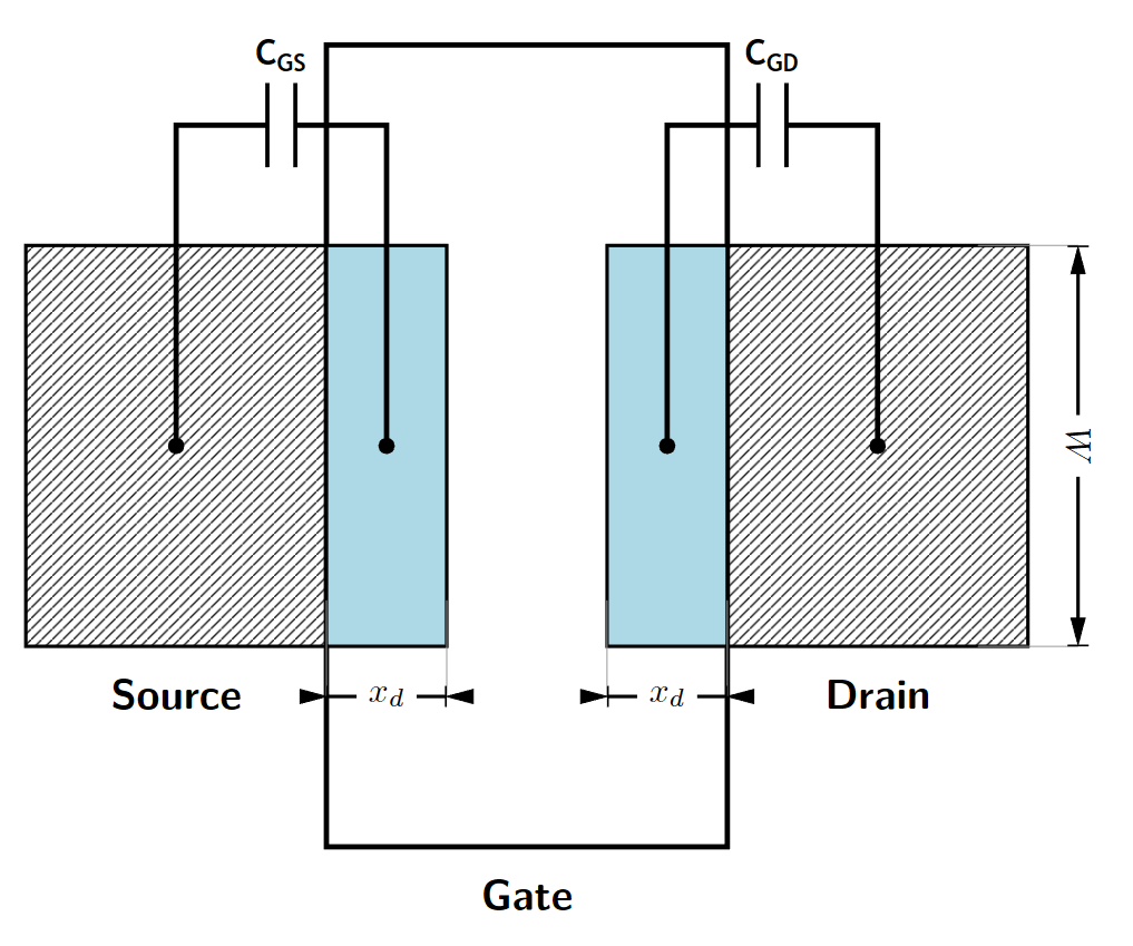
Overlap Capacitances \(C_{GS}\) and \(C_{GD}\)
\(C_{GS}\) and \(C_{GD}\) are overlap capacitances caused by an effective MOS capacitor on the overlap of the G region to the S and D regions.
\[C_{GS} = C_{GD} = \frac{\epsilon_{ox} x_d W}{t_{ox}}\]
But if you may remember…
\[C_{ox}=\frac{\epsilon_{ox}}{t_{ox}}\]
\[C_{GS} = C_{GD} = C_{ox}x_dW\]
The Gate-bulk Capacitance \(C_{gb}\)
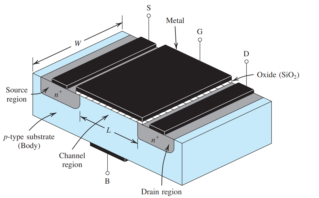
As we discussed before, the main physical device behind the MOSFET is a MOS capacitor.
\[ C_{gb} = \frac{\epsilon_{ox}}{t_{ox}}WL \]
The Drain-bulk and Source-bulk Capacitances \(C_{db}\),\(C_{sb}\)
\(C_{db}\) and \(C_{sb}\) come from junction capacitances of the PN junction formed by the opposite-type semiconductors of the drain/source and the bulk.
MOSFET Capacitances
MOS Parallel Plate Capacitances
- \(C_{gs}\)
- \(C_{gd}\)
- \(C_{gb}\)
S/D-Bulk Junction Capacitances
- \(C_{sb}\)
- \(C_{db}\)
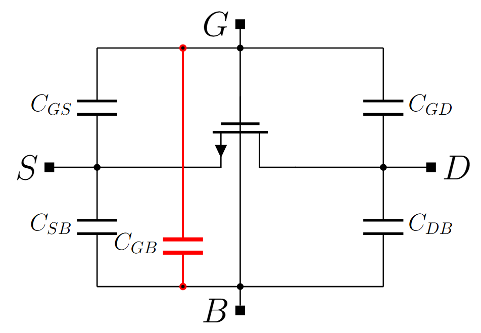
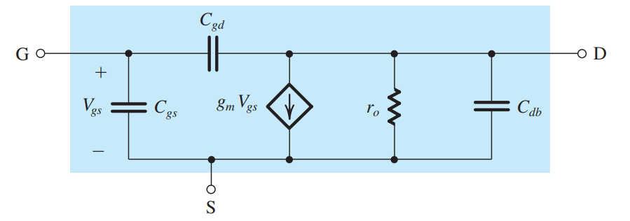
Effective MOS Small-signal with Capacitances
The bulk is typically connected to the source meaning:
\(C_{gs}\) typically also accounts for \(C_{gb}\).
\(C_{sb}\) is shorted.
So, only \(C_{gs}\), \(C_{gd}\) and \(C_{db}\) survive.
The Transition Frequency \(f_T\)
You’ll notice that the current gain reaches 1 (0 dB), but the voltage gain doesn’t.
Hence, people measure the “speed of the transistor” or the transition frequency as \[ \left| \frac{i_o}{i_i} \right|_{f_T} = 1\]

The Transition Frequency \(f_T\)