Frequency Response of CE Amplifier
EEE 131 THX2/Y
2025-11-28
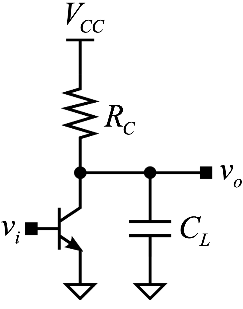
CE Amplifier with an Output Pole
We begin by analyzing the CE amplifier frequency response.
Assumptions:
- Ignore BJT parasitic capacitances (for now).
- Assume \(r_o \rightarrow \infty\).
- An external load capacitance \(C_L\) dominates the output.
CE with Output Poles: \(A_V\)
\[A_v(s) = -g_mR_C \left( \frac{1}{1 + sR_C C_L} \right)\]

CE with Output Pole: \(R_o\)

CE with Output Pole: \(G_m\)

CE with Output Pole: \(Z_i\)

CE Input Impedance \(Z_i\)
\[Z_i = \frac{v_i}{i_i} \bigg|_{v_o=0}\]
By simple inspection of the small signal model: \[Z_i = r_\pi\]
The input impedance is purely resistive and constant across frequency (in this specific configuration).

CE Two-Port Equivalent (Output Pole Only)
We can construct a two-port network representing the amplifier so far:

\[Z_i = r_\pi\]
\[G_m = g_m\]
\[Z_o = \frac{R_C}{1 + sR_C C_L}\]
The CE Amplifier with an Input Pole
Now we add a source resistance \(R_S\) and a base-emitter capacitance \(C_\pi\).

We must determine how \(v_{be}\) relates to \(v_i\) considering the frequency dependent voltage divider at the input.
Magnitude Response (Two Poles)
Typically, the output pole \(\omega_{p2}\) is lower frequency than the input pole \(\omega_{p1}\).

- Flat gain up to \(\omega_{p2}\).
- Slope of \(-20\) dB/dec between \(\omega_{p2}\) and \(\omega_{p1}\).
- Slope of \(-40\) dB/dec after \(\omega_{p1}\).
Phase Response
The phase response depends on the separation of the poles.
\[\angle A_v(\omega) = 180^\circ - \tan^{-1}\left(\frac{\omega}{\omega_{p1}}\right) - \tan^{-1}\left(\frac{\omega}{\omega_{p2}}\right)\]
Widely Separated If poles are far apart, the phase drops in distinct steps. 
Close Proximity If poles are close, the phase shifts merge, creating a steeper descent. 